Metal oxide semiconductor components (Complementary Metal-Oxide Semiconductor (CMOS) image sensor and charge coupled device (ChargeCoupledDevice, CCD) imaging device started almost simultaneously 20 years ago. CCD is a high-end technology component used in photography, and CMOS is used in products with lower image quality.
Because of its advantages of high light sensitivity, low noise, and small pixels, the CCD device has dominated the image sensor market for the past 15 years. In contrast, CMOS image sensors used to have the disadvantages of large pixels, small signal-to-noise ratio, and low resolution. They have been unable to compete with CCD technology. However, with the continuous development of large-scale integrated circuit technology, the technical difficulties that were difficult to solve in the manufacturing process of CMOS image sensors in the past can now find corresponding solutions, thereby greatly improving the image quality of CMOS image sensors.
1. CMOS active pixel sensor
The primary reason why CMOS image sensors have been paid more attention recently is that the sensitivity problem that was much lower than CCD in the past has been gradually solved. Compared with CCD, CMOS sensor has better mass production, and it is easy to implement SoC (SystemonChip) products including other logic circuits, which is difficult to achieve in CCD. In particular, CMoS sensors do not require special manufacturing processes like CCD, so they can directly use production equipment for DRAM and other large-volume products. In this way, it is possible for the CMOS image sensor to form a cost structure that is completely different from the CCD image sensor.
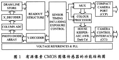
FIG. 1 shows a functional structure diagram of an active pixel CMOS image sensor (ActivePixelSensor, APS), in which the imaging part is a photodiode array (PhotoDiodeArray).
Each pixel of the four-field effect tube (4T) active pixel CMOS image sensor is composed of a photodiode, a reset tube T2, a transfer tube T1, a source follower T3, and a row gate switch tube T4, as shown in FIG. 2.
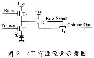
The transfer tube T1 is used to connect the photodiode to the source follower T3, and is connected to VDD through the reset tube T2. The gate of T3 is connected to the N + diffusion region between T1 and T2. Compared with the 3T structure APS, the leakage current effect associated with the gate of T3 is reduced. The role of source follower T3 is to realize the amplification and buffering of the signal and improve the noise problem of APS. T4 is used to connect the signal to the column bus. The working process is: first enter the "reset state", T2 is turned on, reset the photodiode; then enter the "sampling state", T2 is closed, light irradiates the photodiode to generate photo-generated carriers, and the output is amplified by the source follower T3 ; Finally enter the "reading state", then the row gate T4 is opened, the signal is output through the column bus.
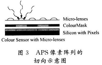
APS has the advantages of low read noise and high read rate, but the pixel unit structure is complex and the fill factor is reduced. The fill factor is generally only 20% to 30%. In order to improve the fill factor of pixels, APS sets up micro-lenses above the pixels, as shown in Figure 3.
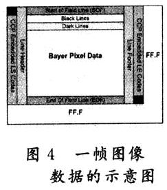
The image information obtained by the APS array is converted into a digital signal by the column analog-to-digital converter (ColumnADC) in FIG. 1, and then undergoes a series of subsequent processing procedures to obtain the output frame image data structure as shown in FIG.
2. Image preprocessing process and method
In order to obtain good image quality, the collected raw image data needs to be processed. Generally, the preprocessing of the image is done in the coprocessor. Recently, with the development of SoC technology, image preprocessing functions can be integrated in CMOS sensors. This is showing the advantages of CMOS image sensors.
The image pre-processing mainly includes a series of processes such as defect correction, FPN noise removal, color difference, image sharpening difference, aperture correction, and gamma correction.
The above image preprocessing process is realized through digital image processing algorithms. The hardware platform may be an image processing circuit integrated in the SoC, an ASIC image processing chip, or a general-purpose DSP chip. The first is to eliminate the defects in the image. If there is a defect in a certain pixel, and its output level is clamped to a high level (black point) or low level (white point), it needs to be compensated by image processing . Usually the average value of the pixels of the same color around it is used to replace the output value of the pixel.
Generally, there are differences in the column analog-to-digital converters of different columns, which leads to the generation of fixed pattern noise (FPN). The data in BlackLines in Figure 4 is used to eliminate FPN. The coprocessor will use this part of data to achieve the purpose of eliminating FPN.
Since each pixel has a certain color filter, it is necessary to obtain the remaining two color information through the color difference. Gamma correction is to eliminate the non-linear effect on the signal transmission between the electrical device and the optical device.
It can be seen from the above image processing process that many algorithms use difference values, which leads to the smoothing of the image, and in order to restore the sharp image, aperture correction is required. In image processing, the sharpened edge obtained by edge detection convolves the smoothed image after the difference to obtain a sharp image.
3. Conclusion
In order to improve the image quality of the CMOS image sensor, this paper proposes a new type of CMOS active pixel image sensor by analyzing the main noise sources and image distortion of the image. The CMOS image sensor uses 4T active pixels, which greatly improves the sensitivity of the image sensor. By integrating the image preprocessing function in the sensor, it has a very good effect on improving the image quality.
Beautiful Wigs Human Hair,Body Wave Hair Wig Human Hair,30 In Lace Frontal Wig
Xu Chang Zhuo YunQing crafts Co., LTD , https://www.wowqueenhair.com